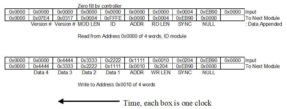
Microprocessor buses are based on address, data, and control lines. Using this type of bus within an FPGA requires constant redesign as you add additional modules for the read multiplexer. In addition, the multiplexer increases in size and complexity as you add each additional component. This method is not optimal for designing within a FPGA.
This bus is based on the idea that the data flows through the modules’ registers in time and is acted upon as required by the message. This method is optimal for an FPGA since no memory and minimal resources are required in each module. The bus is 16 bits wide with a data delay of one clock per module. The default bus speed for the EP2C5 (a very old part) is 50MHz, which provides a bus bandwidth of 100MBytes/second. The bus supports read and write across multiple modules. Each message starts with a null character 0x0000, followed by a sync character 0xEB90. The write message contains the data being written, and a read message has the data appended to the message. The address space for the bus is 16-bit, with 16-bit words (128 Kilobytes). Each block is a minimum of three words long, as shown in the list below.
- First address: Module identification number
- Second address: Module length
- Third address: read or write data
- Fourth through N addresses: read or write data
Each block will pass the data if the address is not within the bounds of the module. Read/write lengths of zero are ignored. At power-up, the interface controller will output a message for each of the modules to auto-define their address. So, the blocks are addressed by their order in the hardware daisy chain. The maximum message size is currently limited to 511 words. There are three message types, as shown below. The read message is zero-padded by the receiver for the number of read words. Note that the interface controller ensures that a zero is always sent before the sync word.
- Auto-define address: 0x0000 (null), 0xEB90 (sync), 0xFE00 (command), 0xAAAA (end address of the last module + 1)
- Read message: 0x0000 (null), 0xEB90 (sync), 0000 000L LLLL LLLL (read with length L in binary), 0xAAAA (start address of read)
- Write message: 0x0000 (null), 0xEB90 (sync), 0000 001L LLLL LLLL (write length L in binary), 0xAAAA (start address), 0xDDDD (data of L words)

Copyright FPGA Magic, 2023